CMOS Sensor
Содержание:
References
- Alexander G. Dickinson et al., «Active pixel sensor and imaging system having differential mode»,
- Zimmermann, Horst (2000). Integrated Silicon Optoelectronics. Springer. ISBN 978-3-540-66662-2.
- ^ Eric R. Fossum (1993), «Active Pixel Sensors: Are CCD’s Dinosaurs?» Proc. SPIE Vol. 1900, p. 2–14, Charge-Coupled Devices and Solid State Optical Sensors III, Morley M. Blouke; Ed.
- , (presented with an award for ‘Seminal contributions to the early years of image sensors’, by the International Image sensor Society in 2015).
- Richard F. Lyon (1981). «The Optical Mouse, and an Architectural Methodology for Smart Digital Sensors». In H. T. Kung; R. Sproull; G. Steele (eds.). CMU Conference on VLSI Structures and Computations. Pittsburgh: Computer Science Press.
- D. Renshaw; P. B. Denyer; G. Wang; M. Lu (1990). «ASIC image sensors». IEEE International Symposium on Circuits and Systems 1990.
- A review of the pinned photodiode for CCD and CMOS image sensors, IEEE J. Electron Devices Society, vol 2(3) pp. 33-43 May 2014 open access
- H. Lin; C.H Lai; Y. C. Ling (2004). «A four transistor CMOS active pixel sensor with high dynamic range operation». IEEE Advanced System Integrated Circuits: 124–127.
- F. Taghibakhsh; k. S. Karim (2007). «Two-Transistor Active Pixel Sensor for High Resolution Large Area Digital X-Ray Imaging». IEEE International Electron Devices Meeting: 1011–1014.
- IEEE TRANSACTIONS ON ELECTRON DEVICES, VOL. 50, NO. 1, JANUARY 2003
История
Схемы КМОП в изобрёл Фрэнк Вонлас (Frank Wanlass) из компании Fairchild Semiconductor, первые микросхемы по технологии КМОП были созданы в . Долгое время КМОП рассматривалась как энергосберегающая, но медленная альтернатива ТТЛ, поэтому микросхемы КМОП нашли применение в электронных часах, калькуляторах и других устройствах с батарейным питанием, где энергопотребление было критичным.
К 1990 году с повышением степени интеграции микросхем встала проблема рассеивания энергии на элементах. В результате технология КМОП оказалась в выигрышном положении. Со временем были достигнуты скорость переключения и плотность монтажа, недостижимые в технологиях, основанных на биполярных транзисторах.
Ранние КМОП-схемы были очень уязвимы к электростатическим разрядам. Сейчас эта проблема в основном решена, но при монтаже КМОП-микросхем рекомендуется принимать меры по снятию электрических зарядов.
Для изготовления затворов в КМОП-ячейках на ранних этапах применялся алюминий. Позже, в связи с появлением так называемой самосовмещённой технологии, которая предусматривала использование затвора не только как конструктивного элемента, но одновременно как маски при получении сток-истоковых областей, в качестве затвора стали применять поликристаллический кремний.
CCDCMOS Image Sensors — 2018
bogotobogo.com site search:
CCD vs CMOS Sensors
An image sensor is a device that converts an optical image into an electronic signal (convert light into electrons).
We have two types of image sensors:
CCD (charge coupled device) image sensor or a CMOS (complementary metal oxide semiconductor) sensor. Both types of sensor accomplish the same task of capturing light and converting it into electrical signals.
Each has unique strengths and weaknesses giving advantages in different applications.
CCDs tend to be used in cameras that focus on high-quality images with lots of pixels and excellent light sensitivity. CMOS sensors traditionally have lower quality, lower resolution and lower sensitivity. CMOS sensors are just now improving to the point where they reach near parity with CCD devices in some applications. CMOS cameras are usually less expensive and have great battery life.
The processes are:
- The sensor used in a digital camera has a 2-D array of thousands or millions of tiny solar cells, each of which transforms the light from one small portion of the image into electrons.
Picture sourse: CCD & CMOS
- Each cell of a CCD image sensor is an analog device. When light strikes the chip it is held as a small electrical charge in each photo sensor. The charges are converted to voltage one pixel at a time as they are read from the chip. Additional circuitry in the camera converts the voltage into digital information.
- A CMOS imaging chip is a type of active pixel sensor made using the CMOS semiconductor process. Extra circuitry next to each photo sensor converts the light energy to a voltage. Additional circuitry on the chip may be included to convert the voltage to digital data.
- Read the value (accumulated charge) of each cell in the image.
- In a CCD device, the charge is actually transported across the chip and read at one corner of the array. An analog-to-digital converter turns each pixel’s value into a digital value.
- In most CMOS devices, there are several transistors at each pixel that amplify and move the charge using more traditional wires. The CMOS approach is more flexible because each pixel can be read individually.
Pros and Cons
It is almost impossible to make a general statement about CMOS versus CCD imagers that applies to all applications. Varied applications have varied requirements.
- CCD camera sensors are very good at capturing light. Because of the way pixels are arranged when compared to CMOS, they tend to perform a lot better in low-light situations.
- CMOS camera sensors, which are less light-sensitive, often have to be compensated for with the introduction of ISO, which introduces noise (grain) to the image.
- CMOS camera sensors have an advantage when facing a white background as CCD camera sensors can present a smearing in brightly lit objects.
- CMOS camera sensors also consume a lot less energy than CCD camera sensors. In fact, this energy consumption is cut down in some cases by a factor of 10.
- CCD camera sensors also have an advantage when it comes to rolling shutter wobble (also known as jellification) when an image is moved or twisted. This wobble is present on CMOS camera sensors due to the rolling shutter, while CCD camera sensors are practically immune to this issue.
- Newer CMOS camera sensors are becoming less sensitive to the movement of a camera as they capture images faster, though they can still present the problem in certain circumstances.
CMOS or CCD ?
Which one?
Some applications are best served by CMOS imagers, some by CCDs.
CMOS camera sensors are cheaper and more energy efficient.
CCD camera sensors are more light sensitive and less prone to rolling shutter wobble.
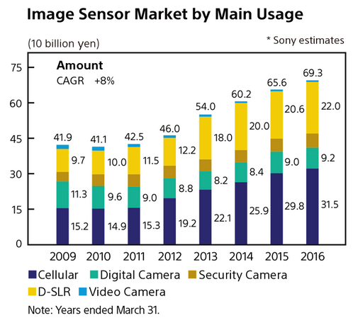
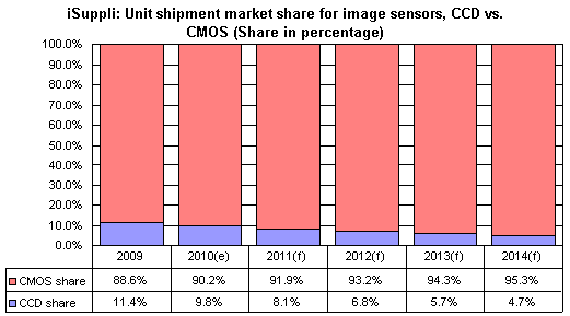
Image Sensor Market
Серии и семейства логических КМОП-микросхем
Серии и семейства логических КМОП-микросхем
- На КМОП-транзисторах (CMOS):
- 4000 — CMOS с питанием от 3 до 15В, 200 нс;
- 4000B — CMOS с питанием от 3 до 18В, 90 нс;
- 74C — семейство в серии 7400, аналогичное 4000B;
- 74HC — высокоскоростное CMOS, по скорости аналогично семействам LS, 12 нс;
- 74HCT — высокоскоростное, совместимо по выходам с биполярными сериями;
- 74AC — улучшенное CMOS, скорость в целом между семействами S и F;
- 74ACT — улучшенное CMOS, совместимо по выходам с биполярными сериями;
- 74AHC — улучшенное высокоскоростное CMOS, втрое быстрее HC;
- 74AHCT — улучшенное высокоскоростное CMOS, совместимо по выходам с биполярными сериями;
- 74ALVC — с низким напряжением питания (1,65 — 3,3В), время срабатывания 2 нс;
- 74AUC — с низким напряжением питания (0,8 — 2,7В), время срабатывания
- 74FC — быстрое CMOS, скорость аналогична F;
- 74FCT — быстрое CMOS, совместимо по выходам с биполярными сериями;
- 74LCX — CMOS с питанием 3В и 5В-совместимыми входами;
- 74LVC — с пониженным напряжением (1,65 — 3,3В) и 5В-совместимыми входами, время срабатывания
- 74LVQ — с пониженным напряжением (3,3В);
- 74LVX — с питанием 3,3В и 5В-совместимыми входами;
- 74VHC — сверхвысокоскоростное CMOS-семейство — быстродействие сравнимо с S;
- 74VHCT — сверхвысокоскоростное CMOS, совместимая по выходам с биполярными сериями;
- 74G — супер-сверхвысокоскоростное для частот выше 1 ГГц, питание 1,65В — 3,3В, 5В-совместимые входы;
-
BiCMOS
- 74BCT — BiCMOS, TTL-совместимые входы, используется для буферов;
- 74ABT — улучшенное BiCMOS-семейство, TTL-совместимые входы, быстрее ACT и BCT;
Для более гибкого применения у ряда производителей существуют также особые семейства, в которых каждая ИМС включает всего 1 логический элемент в 5..6-пиновом корпусе, что бывает полезно для конструкций с малым количеством разных элементов и минимальным размером платы (например: 74LVC1G00GW фирмы NXP; SOT353-1 Single 2-Input Positive-AND Gate)
Серии логических КМОП-микросхем производства СССР
- 164, 176 соответствуют серии 4000, но у 164 и 176 серий номинальное напряжение питания 9 В ±5% (сохраняют работоспособность при 4,5-12 В);
- 561 и 564 — семейству 4000A из серии 4000;
- 1554 — семейству 74AC из серии 7400;
- 1561 — семейству 4000B;
- 1564 — семейству 74HC;
- 1594 — семейству 74ACT;
- 5564 — семейству 74HCT;
- 5584 — семейству 74VНС;
- 5514БЦ — серия логических микросхем на основе БМК. Предназначена для замены устаревших логических микросхем серий564 , 1564 и их зарубежных аналогов.
CMOS and CCD sensors perform similar roles using different technology

Digital cameras are packed with technology.
Insung Choi / Getty Images
Digital Cameras
-
Key Concepts
- Basics
- Guides & Tutorials
- Tips & Tricks
- Tips for Mobile Photography
by
Jo Plumridge
An experienced photography professional and writer for photography and travel venues.
Updated August 13, 2019
45
45 people found this article helpful
All digital cameras have an image sensor that captures information to create a photograph. There are two primary types of image sensors — CMOS and CCD — and each has its advantages.
How Does an Image Sensor Work?
The easiest way to understand the image sensor is to think of it as the equivalent of a piece of film. When the shutter button on a digital camera is depressed, light enters the camera. The image is exposed onto the sensor in the same way that it would be exposed onto a piece of film in a 35mm film camera.
Digital camera sensors consist of pixels that collect photons (energy packets of light) that are converted into an electrical charge by the photodiode. In turn, this information is converted into a digital value by the analog-to-digital converter (ADC), allowing the camera to process the values into the final image.
DSLR cameras and point-and-shoot cameras primarily use two types of image sensors: CMOS and CCD.
What Is a CCD Image Sensor?
Charge Coupled Device sensors convert pixel measurements sequentially using circuitry surrounding the sensor. CCDs use a single amplifier for all the pixels.
CCDs are manufactured in foundries with specialized equipment. This complexity is reflected in their often higher cost.
There are some distinct advantages to a CCD sensor over a CMOS sensor:
- Less noise and typically higher-quality images, particularly in low-light conditions
- Better depth of color because the dynamic range of the sensor is often twice that of CMOS sensors
- Higher resolution and light sensitivity
What Is a CMOS Image Sensor?
Complementary Metal Oxide Semiconductor sensors convert pixel measurements simultaneously, using circuitry on the sensor itself. CMOS sensors use separate amplifiers for each pixel.
CMOS sensors are commonly used in DSLRs because they are faster and cheaper than CCD sensors. Both Nikon and Canon use CMOS sensors in their high-end DSLR cameras.
The CMOS sensor also has its advantages:
- Faster processing speed because the active pixels and ADC are on the same chip
- Lower power consumption, as much as 100 times less than a CCD
- Integrated camera functions like auto exposure, color encoding, and image compression directly in the chip
- Prevents «smearing» when an image is overexposed
- Less expensive manufacturing process
- Quality has improved significantly since their introduction
Color Filter Array Sensors
A color filter array is fitted to the top of the sensor to capture red, green, and blue components of light falling on the sensor. Therefore, each pixel is only able to measure one color. The other two colors are estimated by the sensor based on the surrounding pixels.
While this approach can affect image quality slightly, it is hardly noticeable on today’s high-resolution cameras. Most current DSLRs use this technology.
Foveon Sensors
Human eyes are sensitive to the three primary colors of red, green, and blue, and other colors are worked out by a combination of the primary colors. In film photography, the different primary colors expose the corresponding chemical layer of film.
Similarly, Foveon sensors have three sensor layers, which each measure one of the primary colors. An image is produced by combining these three layers to produce a mosaic of square tiles. This is still a fairly new technology that is in use on some Sigma cameras.
Continue Reading
Design variants
Many different pixel designs have been proposed and fabricated. The standard pixel is the most common because it uses the fewest wires and the fewest, most tightly packed transistors possible for an active pixel. It is important that the active circuitry in a pixel take up as little space as possible to allow more room for the photodetector. High transistor count hurts fill factor, that is, the percentage of the pixel area that is sensitive to light. Pixel size can be traded for desirable qualities such as noise reduction or reduced image lag. Noise is a measure of the accuracy with which the incident light can be measured. Lag occurs when traces of a previous frame remain in future frames, i.e. the pixel is not fully reset. The voltage noise variance in a soft-reset (gate-voltage regulated) pixel is Vn2=kT2C{\displaystyle V_{n}^{2}=kT/2C}, but image lag and fixed pattern noise may be problematic. In rms electrons, the noise is Ne=kTC2q{\displaystyle N_{e}={\frac {\sqrt {kTC/2}}{q}}}.
Hard reset
Operating the pixel via hard reset results in a Johnson–Nyquist noise on the photodiode of Vn2=kTC{\displaystyle V_{n}^{2}=kT/C} or Ne=kTCq{\displaystyle N_{e}={\frac {\sqrt {kTC}}{q}}}, but prevents image lag, sometimes a desirable tradeoff. One way to use hard reset is replace Mrst with a p-type transistor and invert the polarity of the RST signal. The presence of the p-type device reduces fill factor, as extra space is required between p- and n-devices; it also removes the possibility of using the reset transistor as an overflow anti-blooming drain, which is a commonly exploited benefit of the n-type reset FET. Another way to achieve hard reset, with the n-type FET, is to lower the voltage of VRST relative to the on-voltage of RST. This reduction may reduce headroom, or full-well charge capacity, but does not affect fill factor, unless VDD is then routed on a separate wire with its original voltage.
Combinations of hard and soft reset
Techniques such as flushed reset, pseudo-flash reset, and hard-to-soft reset combine soft and hard reset. The details of these methods differ, but the basic idea is the same. First, a hard reset is done, eliminating image lag. Next, a soft reset is done, causing a low noise reset without adding any lag. Pseudo-flash reset requires separating VRST from VDD, while the other two techniques add more complicated column circuitry. Specifically, pseudo-flash reset and hard-to-soft reset both add transistors between the pixel power supplies and the actual VDD. The result is lower headroom, without affecting fill factor.
Active reset
A more radical pixel design is the active-reset pixel. Active reset can result in much lower noise levels. The tradeoff is a complicated reset scheme, as well as either a much larger pixel or extra column-level circuitry.
Architecture
Pixel
A three-transistor active pixel sensor.
The standard CMOS APS pixel today consists of a photodetector (a pinned photodiode), a floating diffusion, a transfer gate, reset gate, selection gate and source-follower readout transistor—the so-called 4T cell. The pinned photodiode was originally used in interline transfer CCDs due to its low dark current and good blue response, and when coupled with the transfer gate, allows complete charge transfer from the pinned photodiode to the floating diffusion (which is further connected to the gate of the read-out transistor) eliminating lag. The use of intrapixel charge transfer can offer lower noise by enabling the use of correlated double sampling (CDS). The Noble 3T pixel is still sometimes used since the fabrication requirements are less complex. The 3T pixel comprises the same elements as the 4T pixel except the transfer gate and the photodiode. The reset transistor, Mrst, acts as a switch to reset the floating diffusion to VRST, which in this case is represented as the gate of the Msf transistor. When the reset transistor is turned on, the photodiode is effectively connected to the power supply, VRST, clearing all integrated charge. Since the reset transistor is n-type, the pixel operates in soft reset. The read-out transistor, Msf, acts as a buffer (specifically, a source follower), an amplifier which allows the pixel voltage to be observed without removing the accumulated charge. Its power supply, VDD, is typically tied to the power supply of the reset transistor VRST. The select transistor, Msel, allows a single row of the pixel array to be read by the read-out electronics. Other innovations of the pixels such as 5T and 6T pixels also exist. By adding extra transistors, functions such as global shutter, as opposed to the more common rolling shutter, are possible. In order to increase the pixel densities, shared-row, four-ways and eight-ways shared read out, and other architectures can be employed. A variant of the 3T active pixel is the Foveon X3 sensor invented by Dick Merrill. In this device, three photodiodes are stacked on top of each other using planar fabrication techniques, each photodiode having its own 3T circuit. Each successive layer acts as a filter for the layer below it shifting the spectrum of absorbed light in successive layers. By deconvolving the response of each layered detector, red, green, and blue signals can be reconstructed.
APS using thin-film transistors
A two-transistor active/passive pixel sensor
For applications such as large-area digital X-ray imaging, thin-film transistors (TFTs) can also be used in APS architecture. However, because of the larger size and lower transconductance gain of TFTs compared with CMOS transistors, it is necessary to have fewer on-pixel TFTs to maintain image resolution and quality at an acceptable level. A two-transistor APS/PPS architecture has been shown to be promising for APS using amorphous silicon TFTs. In the two-transistor APS architecture on the right, TAMP is used as a switched-amplifier integrating functions of both Msf and Msel in the three-transistor APS. This results in reduced transistor counts per pixel, as well as increased pixel transconductance gain. Here, Cpix is the pixel storage capacitance, and it is also used to capacitively couple the addressing pulse of the «Read» to the gate of TAMP for ON-OFF switching. Such pixel readout circuits work best with low capacitance photoconductor detectors such as amorphous selenium.
Array
A typical two-dimensional array of pixels is organized into rows and columns. Pixels in a given row share reset lines, so that a whole row is reset at a time. The row select lines of each pixel in a row are tied together as well. The outputs of each pixel in any given column are tied together. Since only one row is selected at a given time, no competition for the output line occurs. Further amplifier circuitry is typically on a column basis.
Как работают цифровые
Web-камеры
ринцип
работы всех типов цифровых камер примерно одинаков. Рассмотрим типичную схему
наиболее простой Web-камеры, основное отличие которой от других типов камер
— наличие USB-интерфейса для подключения к компьютеру.
Помимо оптической системы (объектива) и светочувствительного ПЗС- или КМОП-сенсора
обязательным является наличие аналого-цифрового преобразователя (АЦП), который
преобразует аналоговые сигналы светочувствительного сенсора в цифровой код.
Кроме того, необходима и система формирования цветного изображения. Еще одним
важным элементом камеры является схема, отвечающая за компрессию данных и подготовку
к передаче в нужном формате. К примеру, в рассматриваемой Web-камере видеоданные
передаются в компьютер по интерфейсу USB, поэтому на ее выходе должен наличествовать
контроллер USB-интерфейса. Структурная схема цифровой камеры изображена на рис.
11.
Аналого-цифровой преобразователь предназначен для дискретизации непрерывного
аналогового сигнала и характеризуется частотой отсчетов, определяющих промежутки
времени, через которые производится замер аналогового сигнала, а также своей
разрядностью. Разрядность АЦП — это количество битов, используемых для представления
каждого отсчета сигнала. Например, если используется 8-разрядный АЦП, то для
представления сигнала используется 8 битов, что позволяет различать 256 градаций
исходного сигнала. При использовании 10-разрядного АЦП имеется возможность различать
уже 1024 различных градаций аналогового сигнала.
Из-за низкой пропускной способности USB 1.1 (всего 12 Мбит/с, из которых Web-камера
использует не более 8 Мбит/с) перед передачей в компьютер данные необходимо
сжимать. Например, при разрешении кадра 320×240 пикселов и глубине цвета 24
бита размер кадра в несжатом виде будет составлять 1,76 Мбит. При ширине полосы
пропускания канала USB 8 Мбит/с максимальная скорость передачи несжатого сигнала
составит всего 4,5 кадров в секунду, а для получения качественного видео необходима
скорость передачи 24 или более кадров в секунду. Таким образом, становится понятно,
что без аппаратного сжатия передаваемой информации нормальное функционирование
камеры невозможно.
Overcoming the problems
CMOS sensors were known for their ‘noise’. In simple terms, this is electrical activity that does not play any part in forming a true image of the subject. One cause of this noise is the individual amplifiers linked to each photo sensor. Inevitably, there are slight variations in output of the millions of amplifiers across the array, and this creates a noise pattern across the image.
Canon has overcome this with lateral thinking. Rather than trying to equalise the amplifiers, it has accepted that there will always be a noise pattern. So every time you take a picture, you actually make two exposures — one of the subject, and one with the shutter closed. This second exposure only captures the noise pattern. If the values of this pattern are subtracted from the first exposure, you obtain an image with little or no noise.
The second main problem with CMOS sensors is also related to the amplifiers, though in a different way. On a CCD, almost all the surface of the unit is occupied by photo sensors. On a CMOS unit, space is needed for amplifier circuitry, so less of the space is given over to the photo sensors. This means that some of the light reaching the unit hits areas between the sensors and is lost, reducing the overall sensitivity of the unit.
There are two solutions to this problem. First, the circuitry can be made smaller and the photo sensors bigger. But there is a limit to this reduction — and an escalation in manufacturing cost — so there will always be space between the sensors. To counteract this, millions of microlenses are used, one over each photo sensor. The microlens covers the photo sensor and the circuitry. Rays of light hitting the edge of the micro lens, which would normally be wasted, are now focused on the photo sensor. The effect is to increase the sensitivity of the sensor unit.
The result is that Canon CMOS sensor units can compete with, and even outperform, CCD sensor units. All current EOS professional digital cameras use CMOS sensor units, and reviews regularly comment on the lack of noise, even at high ISO settings.
Photo sensors on a CMOS unit are positioned inside ‘wells’. Between the wells is circuitry associated with the amplifier units. Rays of light reaching the spaces between the wells are wasted, reducing the efficiency of the CMOS unit.
Placing a micro lens over each sensor and its circuitry captures the light that would normally be wasted and redirects it to the photo sensors.
Схемотехника
Схема логического элемента выполняющего логическую функцию 2И-НЕ
Топология логического элемента 2И-НЕ (схема)
Для примера рассмотрим схему вентиля 2И-НЕ, построенного по технологии КМОП.
- Если на оба входа A и B подан высокий уровень, то оба транзистора снизу на схеме открыты, а оба верхних закрыты, то есть выход соединён с землёй.
- Если хотя бы на один из входов подать низкий уровень, соответствующий транзистор сверху будет открыт, а снизу закрыт. Таким образом, выход будет соединён с напряжением питания и отсоединён от земли.
В схеме нет никаких нагрузочных сопротивлений, поэтому в статическом состоянии через КМОП-схему протекают только токи утечки через закрытые транзисторы, и энергопотребление очень низкое. При переключениях электрическая энергия тратится в основном на заряд емкостей затворов и проводников, так что потребляемая (и рассеиваемая) мощность пропорциональна частоте этих переключений (например, тактовой частоте процессора).
На рисунке с топологией микросхемы 2И-НЕ можно заметить, что в ней используются два двухзатворных полевых транзистора разных конструкций. Верхний двухзатворный полевой транзистор отвечает за формирование высокого уровня на выходе логического элемента, если любой из входов имеет низкий уровень, а нижний двухзатворный полевой транзистор отвечает за формирование низкого уровня на выходе, если оба входа имеют высокий уровень.
Следует отметить, что поскольку переключение n-канальных и p-канальных транзисторов имеет конечное время, на короткое время оба типа транзисторов могут быть открыты и между цепями питания возникает ток короткого замыкания. Это приводит к повышению энергопотребления.
Защита от статического электричества
Так как затворы МДП-транзисторов имеют большое входное сопротивление, электростатический разряд может привести к пробою затвора и выходу микросхемы из строя. Для защиты от статического электричества каждый вывод КМОП-микросхемы оснащают защитной схемой, в которую входят диоды с низким напряжением пробоя, соединяющие каждый вход с шинами питания.
One charge at a time
The tiny photo sensors create only a minute electrical current. This must be amplified before it is of any use in creating an image. Some CCDs have a single amplifier. This deals with the current from each sensor in turn. The amplifier is placed at one corner of the sensor where it reads and amplifies the charge from the nearest sensor in the first row. The charge in this sensor is then released, leaving it ‘empty’. All the charges from each sensor in the first row now move along by one sensor, so that the amplifier can read and process the next charge. This continues until the amplifier has dealt in turn with the charges from each of the sensors in the first row.
At this point, all the sensors in the first row are ‘empty’ of charges. This allows all the charges from the sensors in the second row to move down to the first row. The second row is now empty, and is filled with the charged from the third row. In this way, all the charged drop down a row, leaving the top row empty.
The whole process then repeats itself, with the amplifier dealing with the charges that were originally in the second row.
You can guess the rest. The charges originally in the third row move to the first row, where they are fed one by one into the amplifier. This continues row by row, charge by charge, until the charge from the far end of the top row finally reaches the amplifier.
Of course, the word ‘finally‘ is relative. The whole process takes place very quickly, often in a fraction of a second.
Each charge from the sensor array is ‘tagged’ by the amplifier unit before is passed on to the camera’s microcomputer so that each piece of data can be reassembled in exactly the same sequence to produce the image.
Only five EOS digital cameras use a CCD image sensor, though four of these are not strictly Canon cameras. The EOS DCS3 (July 1995), DCS1 (December 1995), D2000 (March 1998) and D6000 (December 1998) were all produced in collaboration with Kodak. Canon provided the body, but the image sensor and electronics came from Kodak.
There is only one EOS digital camera that uses a CCD in which both body and electronics designed and built by Canon — the EOS-1D (September 2001) — and even here the CCD sensor is outsourced.
The charges (brightness data) from a CCD move across the array photo sensor by photo sensor until they reach the external amplifier unit(s).